The MeiLuft particle Sensor
Detects what is in our air.
What makes our product
so unique?
MeiLuft’s SNIPS (Smart Nano Imaging Particle Sensor) makes it possible to image particles in the range of 100 nm and smaller and to detect them via AI.
Optical microscopes can no longer display particles below 200 nm. However, a virus, ultra-fine dust
or nanoplastics are much smaller, in the range of 100 nm and below.
At the moment, these particles can only be imaged using complex, expensive procedures that can
usually only be carried out in a laboratory. Chemical and biological methods help here, but always
with a loss of detection accuracy and above all the detection rate.
In addition, these methods can only be used very specifically for a particular application.

The development of SNIPS
The following is a brief description of the technical development of SNIPS.
SNIPS ensures the detectability of small particles, for which a resolution in the range of a few nanometres is required in the finished state. The resolution depends essentially on the diameter of the electron beam, whose diameter must be in the same range. To obtain this beam diameter, the beam path of the electrons must be calculated, analogous to the beam path of light in
optical microscopes. The basics for the electrical lenses required for this can accordingly be considered analogous to the calculation of optical lenses. These electrical lenses bundle the electron cloud, starting from the cathode, into a fine electron beam. The basis for the design of these electrostatic lenses are Maxwell’s equations, which are stored in a finite element programme for the
simulation of electron paths. The electron paths follow the electric field lines, which are always perpendicular to the equipotential lines of the electric field.
In the first step, the FEM simulation provides the electrostatic potentials, shown on a simplified lens
system:
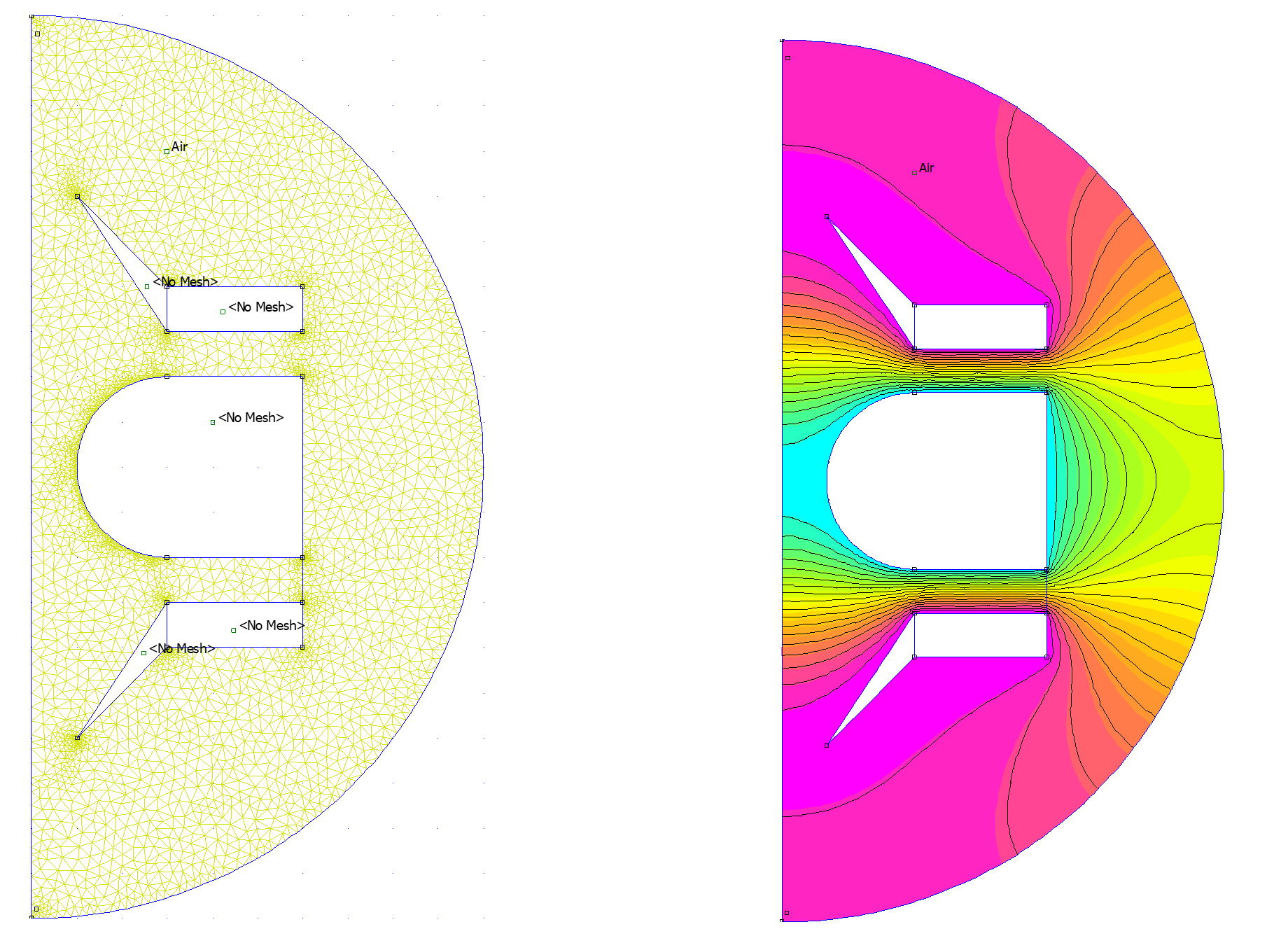
On the left the axially symmetrical 3-electrode lens system, on the right the calculated potential curves.
The potential curve U(Z) on the rotation Z-axis follows from the FEMM calculation in post-processing:
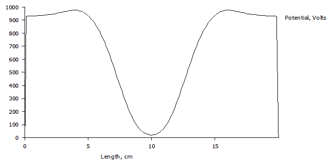
Potential curve U(Z) (ordinate) along the rotation Z-axis (abscissa)
From the potential curve on the Z-axis, the focal length f can now be calculated by polynomial approximation, according to Reimer, as follows:

Based on the simulations, an optimisation process can now be started in which a blasting system is mechanically constructed, which can be seen as a sectional model (in casting compound) in the following figure:
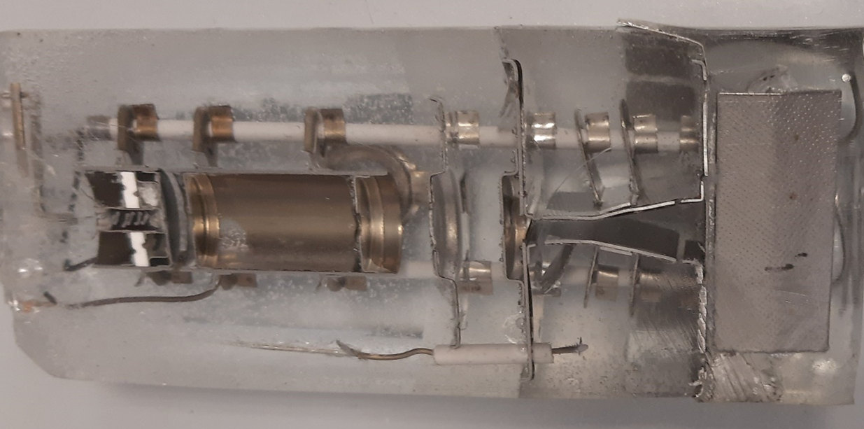
On the left, the incandescent cathode as thermal electron source, followed by the Wehnelt cylinder, annode and focusing lens. On the right edge of the picture, the capacitor plates for the vertical and horizontal beam deflection can still be seen.
The beam system is then tested in a vacuum chamber for its electrical properties in order to optimise the beam system in an iterative process until the desired beam diameter is achieved or the simulation model delivers the desired design at the first attempt.
The following figure shows the setup with the beam system shown in the previous figure in the experiment:
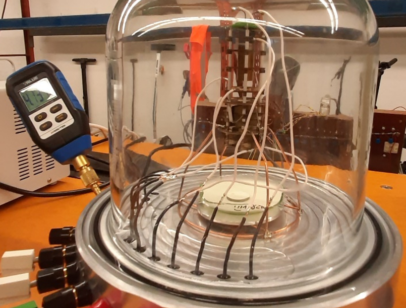
Beam system in recipient bell, with luminescent screen for checking the electron beam diameter
For the complete beam path of a SEM, the cathode, the Wehnelt cylinder and the anode must also be taken into account. The following figure shows an example of the arrangement of these components:
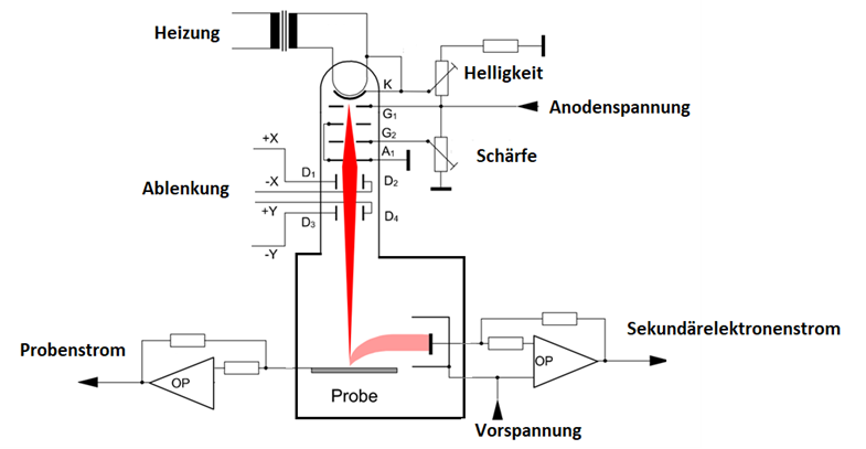
Scanning electron microscope, with electrostatic lens G2, Wehnelt cylinder G1, anode A1 and cathode K. D1 to D4 represent the deflection plates for the beam.